![]()
Frequently Asked Questions (FAQ) - Common Questions to FIDES Guides 2004 and 2009
A:
"Inhabited" shall always be used instead of "habitable".
A:
The same value of C_sensitivity shall be used for both types of tantalum capacitor.
A:
Concerning the table, it should only display "high conductivity" and "low conductivity". Therefore, "conductivity unknown" should be replaced with "high conductivity". Furthermore, if the thermal conductivity of the board is unknown, it is recommended to choose a high conductivity.
A:
If the conductivity is known, there is no problem since a limit value of 15W/m.K has been defined. Otherwise, "low conductivity" generally applies on boards which have surface metallization only (typically for microwave functions). A board which has more than two internal layers (power supply + ground), should be considered as a “high conductivity” board.
A:
Actually, there is a mistake in the table concerning the active components cases: therefore, only six columns should be displayed in the page 61 table (case type, equivalent name, Np, Rjc, Rja with V=0m/s – Low conductivity and Rja with V=0m/s – High conductivity). Rjc “high conductivity” should never be used.
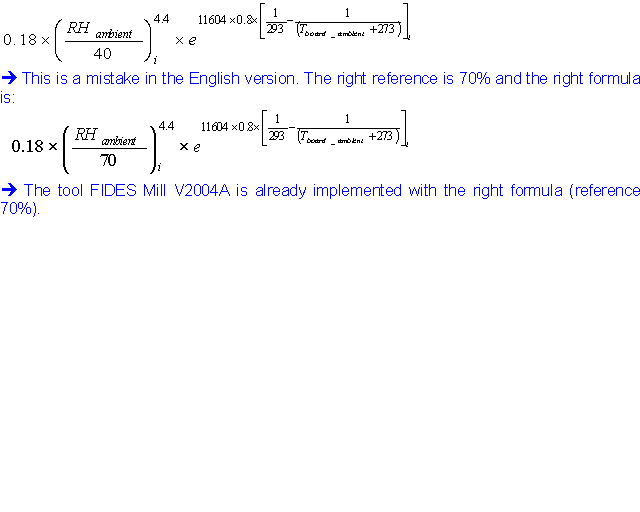
A:
Yes. Unfortunately this is not possible with the current version of FIDES Mill V2004A tool.
A:
This is an inaccuracy. Of course the real applied power has to be taken for Tj calculation and not the rated power.
A:
The definition of the "Routing Class" of PCBs is described in the French standard NF C 93-713. The Routing Class characterizes the density of interconnection (and the tolerances for part placing). The following summary may be used:
| Design values | 1 | 2 | 3 | 4 | 5 | 6 |
| Minimal Width of routed tracks (mm) | 0,80 | 0,50 | 0,31 | 0,21 | 0,15 | 0,12 |
| Minimal spacing between both tracks or pads (mm) | 0,68 | 0,50 | 0,31 | 0,21 | 0,15 | 0,12 |
For a multi-layer PCB, the "Routing Class" is given by the layer with the highest density.
In a same layer, the routed area with the highest density defines the "Routing Class" of the layer.
For a complete definition of routing classes, refer to NF C 93-713.
A:
Yes PCB and connectors remain affected by humidity in operating phases (unlike the other components).